- 邮件
- |

科学研究
团队简介
- 研究员1名副研究员2名
- 高级工程师1名工程师5名
- 博士研究生3名硕士研究生4名
 Research direction
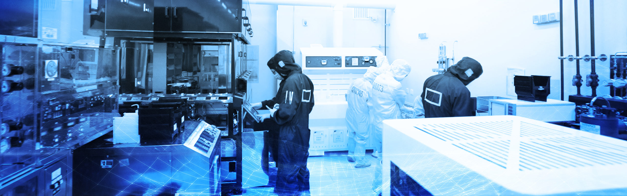
 Hardware conditions
研究方向概况和未来方向
At present, the team has made internationally influential achievements in the epitaxy of high-quality silicon based GaN materials, AlGaN deep UV LEDs and detectors, high-power blue white LEDs and laser material growth, silicon based GaN longitudinal power device epitaxy, 4-8-inch silicon substrate GaN based HEMT electronic material growth, etc. The team has accumulated rich experience in the growth of large size silicon based GaN LED and HEMT materials, has core technology and industrialization capabilities, has applied for dozens of key technology patents in related fields, and has relatively complete independent intellectual property rights.
Next, the team will build the third generation semiconductor material epitaxy research and development center in the Pearl River Delta, and carry out in-depth cooperation with domestic and foreign scientific research institutions and well-known enterprises to provide core material support for the research and development of various high-performance optoelectronic devices and electronic devices, and strive to become a well-known third generation semiconductor epitaxy material supplier in the Pearl River Delta and even at home and abroad. Specifically, we will focus on the following key bottleneck technology breakthroughs:
- 01Epitaxy of large size silicon based GaN RGB tri color LED materials
- 02GaN blue green laser material epitaxy
- 03Epitaxy of aluminum nitride gallium deep ultraviolet optoelectronic materials
- 04GaN RF HEMT and HBT Epitaxy
- 05GaN Power Electronics HEMT and Longitudinal Power Device Epitaxy
- 06Growth of nitrogen polar gallium nitride and quasi van der waals epitaxy
关键领域
The third generation semiconductor materials represented by GaN have significant advantages such as direct band gap, large band gap width, high breakdown field strength, high electron saturation drift rate, high thermal conductivity, etc. It has important application value in the fields of high frequency, high efficiency, high temperature, high power, high withstand voltage, radiation resistance, etc. It is expected to become the pioneer of China's semiconductor industry and technology to overtake at a bend, It has been written into the National "Fourteenth Five Year Plan" and the "Outline of Vision Goals for 2035", and is also the key development object of the Fourteenth Five Year Plan of Guangdong Province. In fact, in recent years, with the rapid development of new displays, 5G communications, the Internet of Things, new energy vehicles and other fields, the market scale of microwave RF devices, power electronic devices, lasers and Micro LED based on GaN materials has expanded dramatically. However, the epitaxial growth of large size and high-quality GaN core device materials is still the key factor limiting its high-end application. Based on this, the team will closely focus on stress regulation, dislocation and point defect suppression, surface/interface engineering, and energy band engineering of large mismatch heteroepitaxial materials, and explore new epitaxial growth technologies such as quasi van der Waals epitaxy, nitrogen polar GaN material epitaxy, to provide core material support for the research and development of high-performance optoelectronics and electronic devices of various nitride semiconductors.
Key research areas - Epitaxy of Large Size Silicon based GaN High Performance RGB Tricolor LED Materials
- High efficiency and high reliability GaN blue-green laser material epitaxy
- Epitaxy of High Efficiency AlGaN Based Ultraviolet Light Emitting Diode Materials
- High frequency and high power silicon based GaN RF electronic material epitaxy
- High efficiency and high power silicon based GaN power electronic material epitaxy
Key application areas - Pixel matrix intelligent vehicle headlights, on-board intelligent light source and head up display
- Wearable electronics and other micro LED new displays, laser displays
- Ultraviolet disinfection and sun blind ultraviolet detection
- 5G mobile communication, radar detection
- Fast charging power supply, electric vehicle and big data center
主要成果和荣誉
The team has presided over a number of scientific research projects, including the national key research and development plan, the key research and development plan of Guangdong Province, and the basic and application foundation of Guangdong Province. The accumulated contract funds have exceeded 70 million yuan. The team is currently working on the flagship physics journal Appl Phys. Let. ACS Appl Mat.&Interfaces, ACS Photonics, CrystEngComm, IEEE Elec. Dev. Let, etc. published more than 30 papers and applied for more than 10 national invention patents.


公众号