

Scientific Research

Compound semiconductor epitaxy
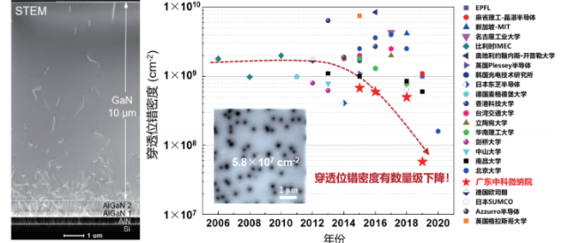
Silicon based GaN heteroepitaxy
Heteroepitaxial growth of gallium nitride (GaN) on silicon substrate is a subversive semiconductor material growth technology. Group III nitride semiconductor devices represented by GaN have unique advantages in low power consumption, small size and high energy efficiency.
AlN heteroepitaxy
Aluminum nitride (AlN) thin film material has the advantages of direct broadband gap, high temperature resistance, radiation resistance, strong piezoelectric effect, etc. It has broad prospects in the field of ultraviolet optoelectronics, power electronics, microwave communications.
Optoelectronic device
Micro-LED
Gallium nitride based Micro LED can greatly reduce the size of the optical machine, significantly improve the light efficiency and dynamic contrast, and has revolutionary alternative prospects in the fields of enhancement and virtual reality, mobile terminal display, vehicle mounted display, etc. due to its advantages such as self illumination, high current density, wide operating temperature range, high output brightness (up to 1000000nit, 30 times OLED), and independent pixel switch.
Ultraviolet optoelectronic device
Aluminum gallium nitrogen (AlGaN) based ultraviolet light emitting diodes (LEDs) cover the 210 – 400 nm band, and have broad application prospects in sterilization, water purification, medical and aesthetic, industrial curing, non direct vision ultraviolet optical communication and other fields.
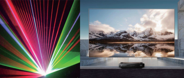
GaN based blue-green laser
GaN based blue and green semiconductor lasers (LD) have excellent monochromaticity, high efficiency, high power density, good directivity and other advantages. As core light sources in projection display, laser processing, laser lighting, storage and undersea communications, atomic clocks and quantum sensors, they have important application prospects and broad market demand.
electronic device
Power electronic device
GaN power devices have the advantages of high breakdown electric field strength, high temperature resistance, high frequency and high efficiency, and will be widely used in consumer electronics, industrial electronics, automotive electronics, national defense and military power conversion fields.
RF electronic devices
GaN RF devices have excellent characteristics such as high frequency, high power, high efficiency, high temperature resistance, radiation resistance, etc. They have significant advantages in the fields of cutting-edge military equipment, civil communication base stations and even 5G mobile terminals in microwave and millimeter wave bands.
Intelligent MEMS devices
Ferroelectric MEMS devices
Ferroelectric MEMS sensors integrate the advantages of ferroelectric materials in radiation resistance, low temperature resistance, high precision material properties and MEMS system advantages, and develop multiple types of ferroelectric MEMS sensors, such as force, heat, sound, light, electricity, which can achieve high-precision in-situ measurement of space environmental parameters in extreme environments such as strong radiation, large temperature difference, and are widely used in aerospace level detection sensors.
High temperature analog chip
High temperature chips can work stably for a long time under the high temperature of 175 ℃, break the foreign embargo, achieve small temperature drift, high-precision signal acquisition, transmission and processing, and have huge market space and prospects in oil drilling and logging, aerospace electronic equipment, heavy industrial process control, generator sets and heavy internal combustion engines.
Time-frequency chip
In order to break the foreign monopoly of clock precision devices, we developed a time-frequency chip with independent property rights, and used silicon based MEMS oscillators, heating elements and temperature sensors to maintain the constant temperature of the working temperature, so that the frequency stability of the time-frequency chip can reach the highest ppb level.
Precision Printing Electronics

Printed capacitance sensor array
Precise capacitive sensor array has the advantages of simple structure, small size, low power consumption, etc. It is a basic component in information fields such as display touch, membrane switch, fingerprint identification, etc. It has a wide range of applications in smart home, biological information identification, consumer electronics and other fields.
Transparent conductive film
Transparent conductive films prepared by printing have the characteristics of both light transmission and conductivity, and are easy to be prepared in large areas, low cost, excellent substrate compatibility, etc. It has become an ideal alternative to ITO electrodes, and is widely used in fields such as PDLC intelligent light adjusting films, OLED information display, thin film photovoltaic cells, and electromagnetic shielding films for transparent windows.
Printed multilayer precision circuit
With the advantages of low cost and large area manufacturing, multi-layer precision circuits prepared by precision printing and manufacturing process have become an important supplement to the material reduction process based on lithography development, and have broad application prospects in the fields of Mini LED circuits, multimodal sensor devices, advanced packaging technology, etc.


Official AC