- 邮件
- |

科学研究

团队简介
Precision printing is the core work of the research group. Through the new process of prefabricated circuit pattern - substrate pattern transfer - ink-jet printing, it is possible to realize the preparation of micron scale electronic circuits based on ink-jet printing; Through the development of functional ink materials, key technical issues such as multi-layer interface function regulation, printable ink optimization, and multi-layer structure accurate overprint were solved to verify the feasibility of printing to prepare high-precision sensor arrays; In combination with the printing process, we can realize large-scale green additive manufacturing of precision electronic circuits. Based on this technology, we will carry out corresponding engineering research on laboratory technology, successfully realize the landing transformation, and meet the market demand of capacitive sensing, electromagnetic shielding, smart home, display, energy and other industries.
研究概况
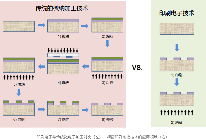
Printing electronic technology is a new electronic manufacturing technology based on the printing process. Compared with the traditional silicon based semiconductor microelectronics technology, the printing electronics technology uses additive manufacturing technology based on solution processing, which has the advantages of simple process flow, low process temperature, flexible processing, green environmental protection, easy mass production and manufacturing (as shown in the figure below), and forms an extremely good technical complementarity with the traditional silicon based microelectronics technology. At present, printed electronics has been applied in new energy, intelligent packaging, intelligent sensor, 5G communication, information display and other fields. It can be predicted that the next 10 years will be a golden period for the development of precision manufacturing technology of printing and electronics in China. Printing and electronics technology will have a significant impact on human production and lifestyle, and may drive the next industrial technology revolution, which will greatly support the country's major strategic plan of "Made in China 2025".
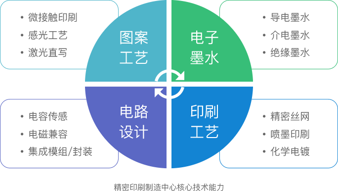
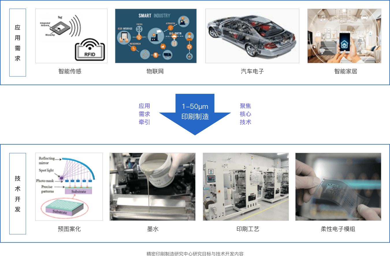
However, due to the characteristics of process equipment and ink spontaneous movement, the precision of traditional printing manufacturing technology is only about 50 microns, which cannot directly meet the preparation requirements of 1-50 microns fine circuits. Aiming at the problem of low precision of current printing and manufacturing technology, the Precision Printing and Manufacturing Engineering Center has designed and carried out research on surface energy difference patterning process, key electronic ink materials, printing process and integrated electronic product development, and strives to achieve large area green additive manufacturing of 1-50 μ m fine electronic functional structure. Based on this key technology, it meets the requirements of information sensing, Internet of Things, automotive electronics Core application requirements such as smart home (see the figure below).
研究方向
A New Process for Preparing Precision Circuits by Pre patterning Printing
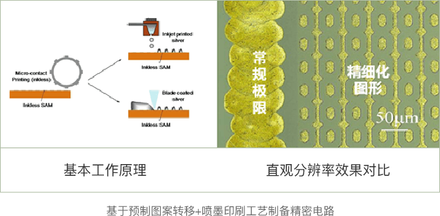
Material pattern transfer - new process of inkjet printing (P3 process), realizing green additive manufacturing based on inkjet printing to prepare micron scale electronic circuits (as shown in the figure). The project team focused on solving such problems as the high fidelity transfer of patterns, the configuration of printable electronic ink, and the preparation process of precision pattern inkjet printing. At present, 4 patents for invention and 2 patents for utility model have been applied, and industrial application transfer has been completed, and verification is being carried out for specific applications.
Development of printable functional ink materials

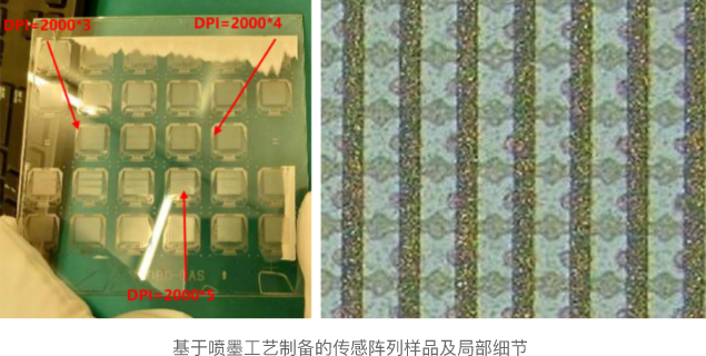
On the basis of improving the circuit printing preparation process, the project team further carried out the research work of functional ink materials, focusing on solving key technical problems such as multi-layer interface function regulation, printable ink optimization, and multi-layer structure accurate overprint. At present, the preparation of 500 DPI sensor array has been realized (as shown in the figure), verifying the feasibility of printing to prepare high-precision sensor array. One utility model patent has been applied for related achievements, and several other patents are in the process of application.
Industrial Application of Precision Printing Manufacturing Technology
Through the research on the printing and preparation process, material development and structure design of ultra-fine conductive patterns, the problem of disconnection between the existing printing electronic technology and industrial chemical and process technology is solved, and the connection between the printing electronic technology products and industrial application needs is realized. At present, the research team has achieved the printing and preparation of a large area of high-temperature resistant transparent electromagnetic shielding film (as shown in the figure), and the developed film products have passed the application verification of users, ensuring the smooth implementation of subsequent industrialization.
联系我们


公众号