

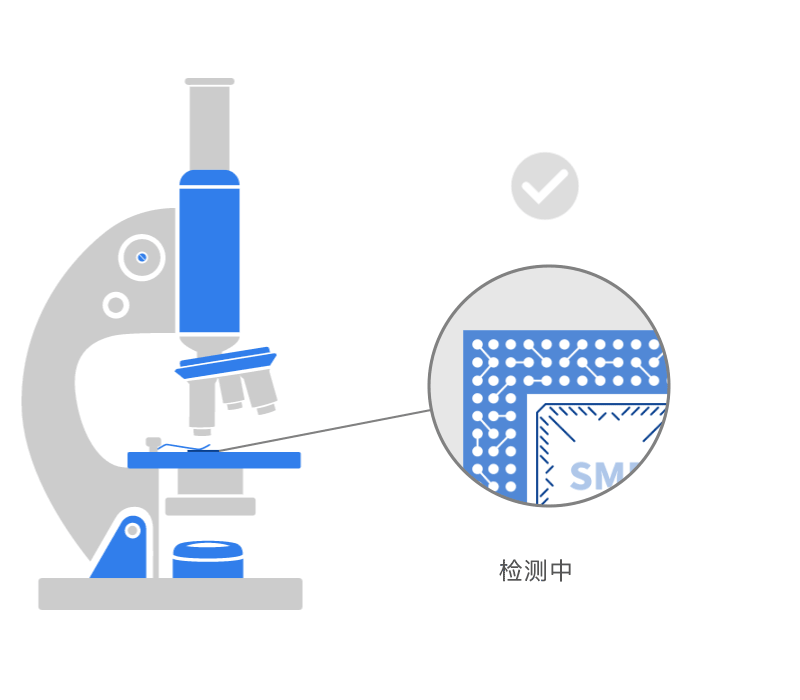
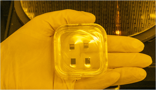
Micro nano processing platform It is a multi-functional public open platform integrating micro/nano manufacturing technology research and development, public services and industrialization. It is planned to build an ultra clean laboratory of about 14000 square meters. It will build a bridge between research and industry with professional teams, advanced equipment technology and perfect infrastructure. It will encircle the processing needs of silicon based MEMS, GaN based chips, biosensors and other chips, and carry out compound material extension for enterprises, universities and institutes The whole process service of Si and GaN based chip manufacturing, packaging and testing covers micro/nano electronics, sensors, optoelectronic devices, power chips, biochips and many other fields.
The micro nano processing platform relies on the rich experience of the processing platform of Suzhou Institute of Nanotechnology, Chinese Academy of Sciences in semiconductor R&D and small scale test services. It is based in Foshan, faces Guangdong, and radiates the Guangdong Hong Kong Macao Bay Area. It focuses on the pilot scale OEM of products 8 inches and below, so that enterprises, universities, and research institutes can focus on the construction of core competitiveness in a low asset and low threshold way, and accelerate to become the leader in the field of technology and industry.
- Professional and shared
Serve customers with professional technical teams and mature semiconductor device processing capabilities, and realize the high openness and sharing of platform resources such as semiconductor equipment and basic processes.
- High quality and efficiency
High quality and high efficiency Provide customers with safe and efficient professional services based on customer demand, high-level technical team, advanced manufacturing management system, customer first service attitude and efficiency first concept.
- Innovation and cooperation
Follow the cutting-edge technology and development trend of semiconductors, and constantly develop new processes and technologies in combination with customer process requirements; Cooperate with relevant enterprises and institutions at home and abroad through joint project application, product cooperative research and development and other forms.
- Round core base
The semiconductor micro/nano processing platform strives to become the preferred base and trusted partner for semiconductor enterprises and institutions to realize their dreams of chips, personnel training and industrial incubation.
8-inch MEMS processing line
Meet the requirements of smart chip manufacturing applications8-inch Micro LED, 8-inch HEMT processing line
Meet the needs of display, optical communication and power electronics industriesPhotoelectric device processing line
Meet the needs of UV and laser industries8-inch biomedical chip processing line
Meet the needs of medical and health industries
8 inch pilot foundry
Utilize existing technologies to provide customers with one-step, short process, whole process and other pilot OEM services
Demonstration application of semiconductor equipment and consumables
Evaluate the products of domestic and foreign semiconductor equipment and material manufacturers, promote and try them through cooperation on the platform, and constantly improve product design and user experience

Service mode

Pilot research and development and technical consultation
Evaluate according to customer needs, develop independently by the customer, develop with the assistance of the platform, and determine the final process plan; Help customers find and solve problems in chip processing
Subcontracting
According to customer needs, provide technical processing plans and provide full process services for device processing and testing

personnel training
Organize theoretical study and technical training for micro nano processing technology of semiconductor devices; Cooperate with enterprises and universities to carry out professional training and practical learning01
Photolithography
It has a variety of lithography auxiliary equipment, such as double-sided ultraviolet lithography machine, DUV lithography machine, multiple models of step lithography machine and matching adhesive coating developer, isolationary daughter cleaning machine, HMDS oven, etc., which can meet the requirements of 4-inch, 6-inch, 8-inch wafer lithography process
- Exposure resolution: 130nm-800nm
- Wafer size: 8-inch downward compatible

02
Coating
It has plasma enhanced chemical vapor deposition (PECVD), low pressure chemical vapor deposition (LPCVD), inductively coupled plasma chemical vapor deposition (ICPCVD), atomic layer deposition (ALD), multi chamber magnetron sputtering, electron beam evaporation table and other coating equipment, compatible with 8-inch and below wafers
- Available materials:
1. Ti, Al, Cu, Au, Cr, Pt, Ag, Mo, W, TiW, AuGe and other metal and alloy films
2. poly Si, a-Si, SiO2, SiNx, TEOS SiO2, ITO, Al2O3, TiO22, TiN, AlN

03
Etching
It has reactive ion etching (RIE), inductively coupled plasma (ICP), ion beam etching (IBE), wet etching and other types of etching equipment, and is compatible with 8-inch and below etching processes
- Etching materials:
Si, SiO2, SiNx, a-Si, polysilicon, Au, Al, Cr, Ti, W, GaN, ITO, etc.

04
Injection
It has medium beam ion implanter equipment, which is compatible with the doping process of 8 inches and below, and has small doping depth (1 μ M), doping is not limited by the equilibrium solid solubility
- Injected energy: 1keV-750keV
- Injected dose: 1E11 ~ 1E15 ions/cm2
- Injected elements: B, P, F, Al, N, Ar, Mg, H, Si, etc.

05
Encapsulation
It has chemical mechanical polishing machine (CMP), bonding alignment machine, temporary wafer bonding machine, permanent wafer bonding machine, high pressure wafer bonding machine, silicon wafer cutting machine, and packaging equipment compatible with 6-inch and 8-inch wafers such as bonding, cutting, and thinning.

06
Testing
It has field emission scanning electron microscope (FESEM), stress meter, ellipsometer, step meter, film thickness meter and other types of testing equipment.
07
Heat Treatment
It has rapid annealing furnace, tubular furnace and other types of heat treatment equipment, compatible with 8 inch and below wafers
- Parameters of rapid annealing furnace:
Maximum temperature: 1250 ℃
Maximum heating rate: ≤ 30 ℃/sec for pure SiC disk
Process atmosphere: N2, Ar, O2
08
Auxiliary Process
The company has high temperature oxygen free oven, vacuum oven, gold spraying instrument, sand blasting machine and other equipment.

Semiconductor chips are mainly divided into integrated circuits, discrete devices, optoelectronic devices and sensors according to their structures and functions. According to different functional materials of chips, semiconductor chips can be divided into silicon based and compound semiconductors. Chip manufacturing generally goes through wafer processing, material epitaxy, photolithography, coating, etching, ion implantation, packaging, testing and other steps. Different process steps are combined and repeated according to chip functions to form specific material growth and structure manufacturing to achieve device performance.
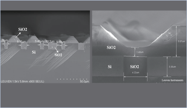
Si high aspect ratio etching process
It has the high aspect ratio etching process capability of Si materials, and has mature Bosch process and non Bosch process. The related processes are widely used in Si based MEMS sensors, TSV 3D packaging, shallow isolation grooves between MOSFET and DRAM cells, etc.
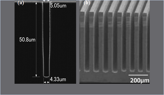
SEM of deep Si etching process: (a) non Bosch process; (b) - (c) Bosch process
GaN Low Damage Etching Process
It has the ability to etch GaN, p-GaN, AlGaN and other Ⅲ - Ⅴ compound materials, realizes the rapid etching and low damage etching process of GaN, and is compatible with the atomic layer etching (ALE) process of AlGaN. The related processes are widely used in the Mesa etching, isolation etching, gate etching and other aspects of GaN based optoelectronic devices.
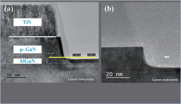
SEM diagram of ICP etching GaN: (a) p-GaN and AlGaN etching results; (b) AlGaN Etching Low Damage Process
Ion beam etching process
Able to etch SiO2, SiNx, Al, Au, Ti, Pt, ITO and other materials, the tilt angle of the platform is - 90 °~80 °, and the uniformity within/between chips/between batches is ≤ 5%. The related processes are widely used in materials and metals that are difficult to etch, Pt thin film temperature sensors, piezoelectricity of radio frequency MEMS (SAW/FBAR/BAW), and complex magnetic materials (AMR/GMR, TMR/MRAM) of mixed metal dielectric materials by electrode etching.
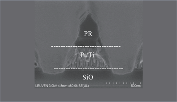
SEM Diagram of Pt/Ti Etched by IBE
Wafer bonding process
Based on the anodic bonding process, the bonding between Si wafer/Si wafer with surface pattern structure and glass can be realized. The bonding pressure can be controlled at 0-20KN, the temperature is 0-450 ℃, the voltage is 0-2000V, and the pattern alignment error after bonding is ≤± 3 μ m。 Au Au bonding, Au Sn, Ge Al bonding can be realized based on hot pressing bonding process. The bonding pressure can be controlled at 0-100KN, the temperature is 0-550 ℃, and the alignment accuracy after bonding is ≤± 5 μ m。
High power GaN semiconductor laser lamp
Stealth cutting process
High precision and nondestructive cutting capability for Si materials. Invisible cutting is to break the Si material inside the wafer by infrared laser, forming a damage layer, and achieve high-precision wafer cutting. It can realize damage free cutting of Si wafer surface. Wafer cutting thickness can reach 750 μ m. The cutting speed reaches 800mm/s.
Optical micrograph of invisible cutting process
Photolithography
Step projection lithography machine Lithography pattern Contact UV lithography machine can achieve the minimum exposure resolution of 800nm, and the overlay accuracy is ± 1 μ m ; The DUV lithography machine can achieve the minimum exposure resolution of 130nm for 8-inch wafers, and the nesting accuracy is ± 25nm; The step projection lithography machine can achieve the minimum exposure resolution of 450nm, and the nesting accuracy is ± 100nm, meeting the requirements of 4-inch, 6-inch and 8-inch wafer lithography processes.

Photolithography of step projection lithography machine
GaN Micro LED process
Epitaxial growth of 6-inch Si based GaN LED material, 256 × 192(15 μ M pixel pitch) passive micro display chip, 2560 × 1920 ultra-high resolution red, green and blue monochrome micro display chip process development, the pixel density can reach 5000 ppi, pixel spacing 5 microns. A complete process flow for preparing 8-inch high resolution chips is formed by directly bonding 8-inch Si substrate GaN Micro LED epitaxial wafers with 8-inch Si based CMOS micro display drive wafers. Single red, green and blue full-color image display is realized by quantum dot lithography technology, and full-color Micro LED is successfully applied to small volume near eye display module.
8-inch Micro LED micro display wafer
GaN based enhanced HEMT device process
The problem of p-GaN etching damage and precise control is solved by using H-plasma to treat p-GaN enhanced power electronic devices. At present, 50 mm gate width p-GaN gate enhanced GaN HEMT has been prepared, the threshold voltage is 2.3 V (defined by the maximum transconductance method), and the maximum drain current ID is 13.7A@VGS =6V (274 mA/mm), the maximum transconductance Gm is 4.7S@VGS =3.9V (94 mS/mm), the threshold hysteresis of forward and reverse scanning is only 45 mV, the switching ratio reaches~109, the ON resistance RON is 235 m Ω (11.75 Ω• mm), and there is almost no hysteresis in forward and reverse scanning. 850V off state voltage, leakage current 0.01 µ A/mm.
GaN based enhanced HEMT device
Low temperature high quality medium film deposition process
It has a low temperature (20~180 ℃) deposition process for SiO2, SiNX, amorphous silicon and other materials. The deposition rate of SiO2and SiNX can be ≥ 15nm/min, the absolute value of film stress can reach SiO2≤ 300MPa and SiNX ≤ 500MPa, and the BOE corrosion rate (BOE (7/1) @ RT): SiO2≤ 300nm/min; SiNX ≤ 50nm/min, homogeneity within and between tablets<± 5%. The related processes have been widely used in low temperature deposition, micro groove filling, MEMS pressure sensors, GaN based optoelectronic devices, etc. for peel off technology.
SEM Diagram of ICPCVD Micron Groove Filling SiO2Process
Complaints and feedback
- Email: dszhao2019@sinanogd.ac.cn
- Tel: 0757-88591811
technical advice
- Email: jgpt@sinanogd.ac.cn
- Tel: 0757-88591819


